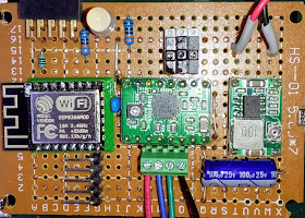
I plan to make a few projects based around ESP-12F WiFi modules. These are postage stamp sized modules containing an ESP8266 chip plus 4MB of flash. The ESP8266 chip is a 32 bit MCU with an integrated WiFi transceiver and TCP/IP stack. They come programmed as a WiFi modem but they can be reprogrammed with the Arduino IDE to do other things in addition to the WiFi. Great for IOT applications because they are so small and cheap (less than £2) but reasonably powerful. A lot more powerful than an Arduino, for example, but with less I/O.
The solder pads are on a 2mm pitch, so they are often used with a breakout board to adapt them to 0.1" pitch for breadboard or perfboard, etc. That adds cost and increases the size somewhat because the through hole pins need to be outside the perimeter of the module. I solved the problem another way, by using a 3D printed wire guide that routes wires from the 0.2mm pitch holes to the nearest 0.1" hole, minimising the space used and costing virtually nothing.
The holes in the module are quite small so I use stripped wire wrap wire. I push it through the module, down through the guide, which routes it to the correct hole in the perfboard. I fold the top over, solder it to the module and trim it. I do the four corners first and pull them tight and solder underneath to secure the module.
Here is a module mounted on perboard.
It doesn't use any extra board space outside the 0.1" holes it uses. I.e. the adjacent holes are all usable.
I didn't break out the end connections because they are not very useful. They are all GPIO lines used internally for the flash. I read it is possible to free up two by removing the can and re-configuring the flash chip to use a two bit interface instead of four bits, but that is too much hassle for me.
Here is the OpenSCAD that produced the adapter: -
The only notable thing is the squeezed wall definition, see my previous post.


No comments:
Post a Comment