To put the ESP8266 into serial programming mode it needs to be reset with GPIO 2 held high, GPIO 15 low and GPIO 0 low. On the other hand to start it executing flash GPIO 0 needs to be high during reset. I have seen lots of circuits on the web, for example the NodeMCU board and Adafruit's Huzzah board that pull GPIO 0 to ground with a switch and / or with DTR from a USB to serial adapter. Reset can be driven from RTS to automate programming with the Arduino IDE.
A lesser known fact is that when the ESP8266 goes into programming mode it outputs a 26 MHz clock on GPIO 0 with considerable drive strength and fast edges. Shorting this to ground or DTR is not good at all as it causes massive contention and generates a lot of noise. This can cause programming to fail unless there is some hefty decoupling on the supply rail. The simple solution is to put a resistor between GPIO 0 and whatever is pulling it low. Here is what the signals look like with 10K between GPIO 0 and DTR from an FTD1232.
The oscillation doesn't show up at full amplitude with a slow time base but I can assure you it is full swing with plenty of overshoot due to not being terminated. You can see a bit of it coupled onto the TX line and this is when it is through 10K. Imagine how noisy things get when it is fighting with the FTD1232 DTR line and winning.
Another lesser know fact is that when the ESP8266 is in reset its GPIO lines get pulled up internally. You can see with 10K pulling it down the GPIO line only goes down to about 0.7V during reset.
Before reset my application is driving GPIO 0 low. RTS goes low a short time before DTR, so it briefly becomes an input and gets pulled to 3.3V by DTR before it pulls it low again. This explains the spike on the left.
I haven't seen any circuits published that avoid this contention.
Sunday, 15 April 2018
Tuesday, 3 April 2018
Printed ESP-12 module breakout adapter
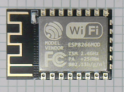
I plan to make a few projects based around ESP-12F WiFi modules. These are postage stamp sized modules containing an ESP8266 chip plus 4MB of flash. The ESP8266 chip is a 32 bit MCU with an integrated WiFi transceiver and TCP/IP stack. They come programmed as a WiFi modem but they can be reprogrammed with the Arduino IDE to do other things in addition to the WiFi. Great for IOT applications because they are so small and cheap (less than £2) but reasonably powerful. A lot more powerful than an Arduino, for example, but with less I/O.
The solder pads are on a 2mm pitch, so they are often used with a breakout board to adapt them to 0.1" pitch for breadboard or perfboard, etc. That adds cost and increases the size somewhat because the through hole pins need to be outside the perimeter of the module. I solved the problem another way, by using a 3D printed wire guide that routes wires from the 0.2mm pitch holes to the nearest 0.1" hole, minimising the space used and costing virtually nothing.
The holes in the module are quite small so I use stripped wire wrap wire. I push it through the module, down through the guide, which routes it to the correct hole in the perfboard. I fold the top over, solder it to the module and trim it. I do the four corners first and pull them tight and solder underneath to secure the module.
Here is a module mounted on perboard.
It doesn't use any extra board space outside the 0.1" holes it uses. I.e. the adjacent holes are all usable.
I didn't break out the end connections because they are not very useful. They are all GPIO lines used internally for the flash. I read it is possible to free up two by removing the can and re-configuring the flash chip to use a two bit interface instead of four bits, but that is too much hassle for me.
Here is the OpenSCAD that produced the adapter: -
The only notable thing is the squeezed wall definition, see my previous post.
Subscribe to:
Comments (Atom)


